
Extreme Demands on Speed and Precision
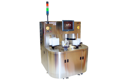
Waferlase ID systems are designed to meet the most stringent requirements of silicon wafer marking, assuring traceability ón the manufacturing process of semiconductor devices. The systems all produce marks that are machine-readable, have no negative influence on subsequent manufacturing steps and still permit clear identification at the end of the process chain. Waferlase ID systems produce debris-free marks suitable for the most extreme cleanroom environments.
The Waferlase ID system is available as Waferlase ID 200 suitable for silicon wafer ID marking up to 200 mm wafer sizes and as Waferlase ID LED especially for traceability of LED devices.
Features at a glance
- small footprint
- open-cassette
- low-maintenance
- fault-free operations suitable for clean-room environments
- field proven beam steering electronics for high accuracy and repeatability
- dual-arm wafer-swapping Pick-n-Place robot with electronic pre-aligner
Dimensions (W x D x H) [mm]: | 1270 x 1600 x 2151 |