
For IGBT Annealing and Wafer Marking
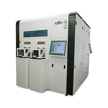
The new laser wafer processing system Waferlase® 200/300/450 is the industrial turnkey solution for front-end-of-line (FEOL) processing for the SEMI industry.
The fully automated modular system comprises a market-leading handling system for (ultra) thin semiconductor wafers and a choice of laser processing modules for laser marking or IGBT laser annealing.
The integrated top-notch wafer handling technology provides precise, non-contact transportation of ultra-thin wafers, even with considerable warpage and bow. The system comes with two or more cassette ports for Open Cassette or FOUP wafer carrier systems.
Features
- Complete all-in-one solution for the SEMI industry
- From process to final product
- IGBT annealing with highest activation rate
- Debris-free marking with controlled marking depth below 1 μm up to 7 μm
Customer Benefits
- Open cassette and/or FOUP wafer carrier systems
- Fully SEMI standard compliant